I want to design a board based around the Gowin littlebee FPGA I think it is going to be the GW1NSE-C2 which has an embedded ARM Cortex M4 processing core. So deep into the datasheet jungle, I go and start designing a board. After much reading, I realize that is going to need a JTAG programmer of some type. so after much research, I find a project for as low-cost JTAG programmer based on an MCU from WCH who also makes a low-cost USB->UART chip which I have looked at in the past. So this sparks off another PCB project, SimpleJTAG.
Somewhere in the middle of this, I run into the low-cost RISC-V MCU's from Gigadevice and with a fascination in RISC-V and a new JTAG programmer on the horizon I start investigating how to source these. Is everyone still with me :)?
Back to the FPGA project, I started with so now I have a JTAG programmer on the horizon and maybe another MCU board not even going to mention the Tindie shop (yes another thing I'm working on). I dive into Gowin's EDA tool for configuring their chips. After much poking around in the dark I find out how to activate the ARM core and become totally lost as I am made aware of my huge gaps in my knowledge when it comes to SOC architecture. Though there is an ARM core on this chip all the flash, ram and peripherals need to be configured inside the FPGA fabric and with the choice of either Verilog or VHDL to program this in I discovered in need a better understanding of computing architecture.
This is where I run into a video series from 'The 8-Bit Guy' on the history of commodore computers with some really nice detail on the system architecture. So to solve the gaps in my knowledge its time to design and build an 8-bit computer from the 80's.
Why make something so outdated?
The early home computers have a very straightforward system architecture ROM, RAM, and peripherals. I can understand the system as a whole and can break it down into constituent parts. Modern hardware has so much integrated that there is no chance of having a complete understanding. Also, there is a big nostalgia factor I can remember going to my neighbors and loading games into is ZX spectrum and using my brothers ZX+3 while he was out and writing early programs in basic.
Of course, the first task ahead it to try and pick a processor for this design (MPU) I need something simple which old acts a processing unit if it contained its own ROM or RAM then I would defeat the process of the learning system architecture. I looked at both the Zilog Z80 and the MOS6502 as possible options, then I ran into ubiquitous almost forgotten Motorola MC6800 which proceeded the other two by a couple of years.
The first look at the datasheet of the MC6800 I was slightly put off with the clocking requirements. It required two clock signals.

The signals are not quite inverse to each other and would require additional hardware to generate. There is a single chip clock generator also made by Motorola the MC6875 but after a quick search it seems to be quite rare and at over $10 e a bit rich for me.
But then I found a later version of the same processor the MC6809 which had some extra features and had the clock generator internal to the IC and only requires an external xtal to run it.
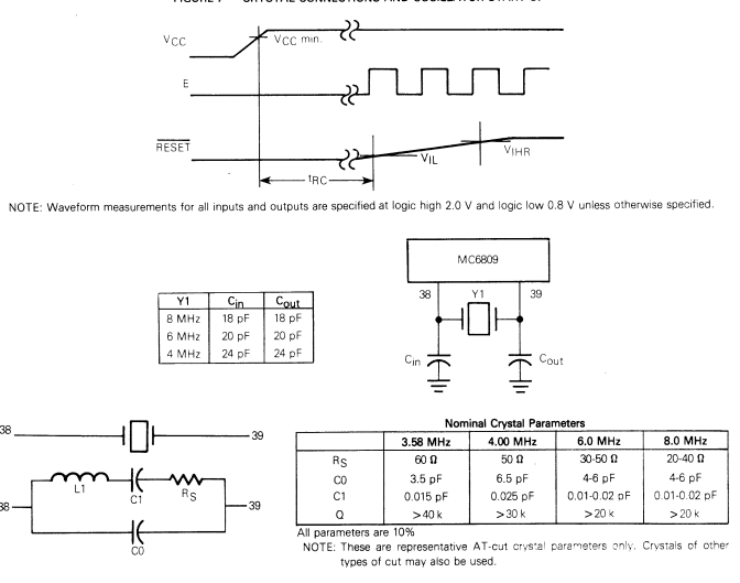
This was the MPU I was going to use. I found a similar project which gave me some initial guidance. https://sites.google.com/site/gogleoops/mc6809-min-board Which is giving me a lot of direction when it comes to working out address select logic and how bus timing and R/W.
So the first board its basic structure looks like this.

I found an online assembler and debugger which seems pretty good
The compiler has options to step through the program and see how it operates its really shown me the specifics when it comes to what the Reset Vector is (I thought it had the first instruction but in fact, it is a memory address which is written to the program counter where the first instruction is located). Also how the stack pointer works with subroutines and how easy it is to cause a stack overflow :).
I have routed the first revision of this board I think it looks pretty good.

I decided to go for a mix of surface mount and through-hole parts as this project is just for me o don't see myself making huge numbers of them.
Updates on this project can be found on Hackaday.io
https://hackaday.io/project/170307-basic-mc6800-interface-board