USB-C is more and more becoming a standard in the maker community for power supply and coms with peoples creations. But there is a catch to this although the USB A plug to USB C plug cable is freely available almost everywhere, the sockets can be a little more daunting. There are not only many to choose for including some with and without through-hole pin the pitch and spacing often means you have to spin a PCB to make them work. then there are concerns with soldering them effectively.
I started to wonder if this would be possible with a USB-C socket with one edge of the PCB inserting into the USB-C plug connector directly. I did a quick Google search and was very surprised that this seemed as though it hadn't been done before. 😏
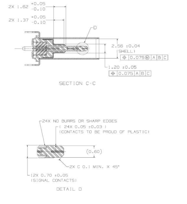
And there it was the "tongue" of the USB-C receptacle is 0.6mm wide wit the contacts proud of the Plastic or in my case PCB.
Wondered if 0.6mm PCB would break the bank in production costs so it was time to have a search around. My usual stop now for PCBs is
JLCPCB. Is I went and had a quick look to see that it wouldn't cost the earth to at least experiment and see if this is viable.
Surprising enough that even with a lead-free finish it would only cost £6 including shipping, at least to do some experimenting.
Even if I ordered V-cut panels which would give me 90+ pieces they would cost less than £0.13 each.
It was slightly shocked at how the price jumped when I selected my usual black solder mask finish, with a large "Special Process Fee". That would certainly blow the budget feels like I'm ordering boards in 2013 again 😅. Looks as though I want to be able to sell these at a reasonable price then they will have to be green.
With my mind made up it was back to the USB-C spec sheet.
Time to fire up KiCAD and get on with creating the part.
It took a bit of drawing but here is. there is something that I found frustrating within KiCAD. this is I couldn't find a way to draw on the edge cut layer in the footprint editor. Not entirely sure if it is something I missed but decided to draw the board edge into the user drawing layer that I can copy over later.
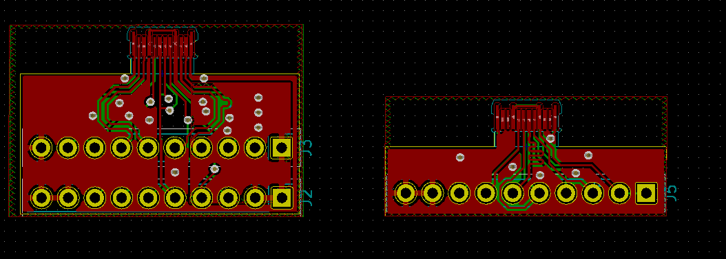
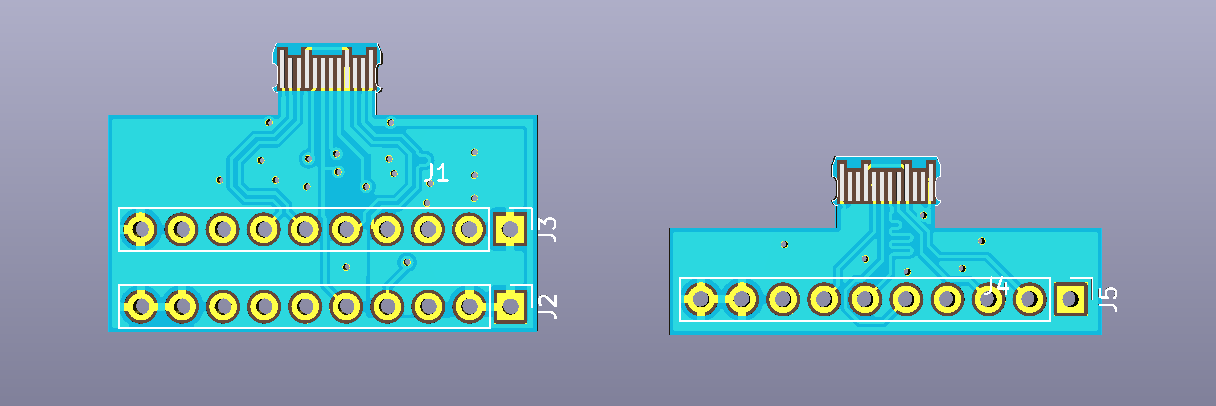
At the end of the day, I just want to see if this is a workable design so decided that making a breakout is the best plan.
So far I have done two designs the one on the left has all 24 pins broken out for USB-SS and the right one is just for up to USB-HS. All the highspeed lined have their differential traces matched in length but the SS traced don't have the required supporting hardware, caps and filtering etc.
It was around this time i started to tell people what I was up to at which point I found there have been a few previous attempts at this type of connector.
I'm not put off exploring this path however I still think this could be a viable option could do with some tweaks in the long run. The other reason for continuing this is I don't think this option has been completely explored of documented yet.
At this point, I'm making some final tweaks to this design and hopefully sending off for production next month.
If you are interested in exploring this concept yourself all my Kicad files are available on Github so feel free to use them as you desire.
Footprint file: https://github.com/rabid-inventor/Kicad-assets/blob/master/footprint.pretty/usb-c-pcb.kicad_mod
Breakout Design: https://github.com/rabid-inventor/UBSC_PCB_Socket_Adaptor