CHUSBIE552

Thursday 13 December 2018

BAW: Update

FIRST OF ALL


Hi all,

I feel its about time I gave everyone who reads this blog a bit of an update on what is happening with board a week.

I think the first thing i have to really say is that I am still designing boards on a semi regular basis I still have much to learn and want to continue making boards.

I think one thing I i have had to except is that currently I am not able to design a board a week, and I is not due to drive to do it. I have other responsibilities that need to be met first whether that is to my family, my work or just to have a little time for myself. The hard thing is to admit is I can't do it all even though I try.

I think the other think I have to keep in mind is not to be too hard on myself about all of this, I think just making little strides towards getting something completed is as good as going heavily from start to finish and being frustrated when  I can't achieve this goal. I think I discovered that in week 4 trying to complete the bubble watch in one straight run proved not to work. that one i will come back to soon. I the meantime i have learnt far more about the STM32 platform which will allow me to go back and complete it. 

WHERE I AM NOW


As BAW is at the moment I'm putting the finishing touches to Week 9 M0GO a USB Device Dev Board. I think after that it will be a revisit to Bubble Watch.

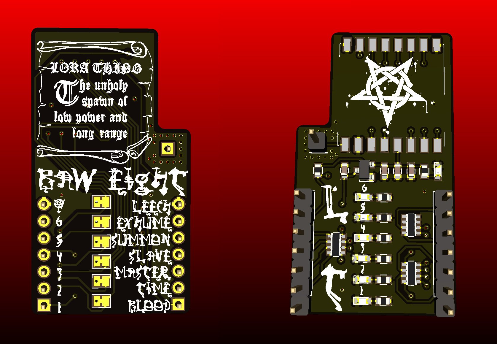
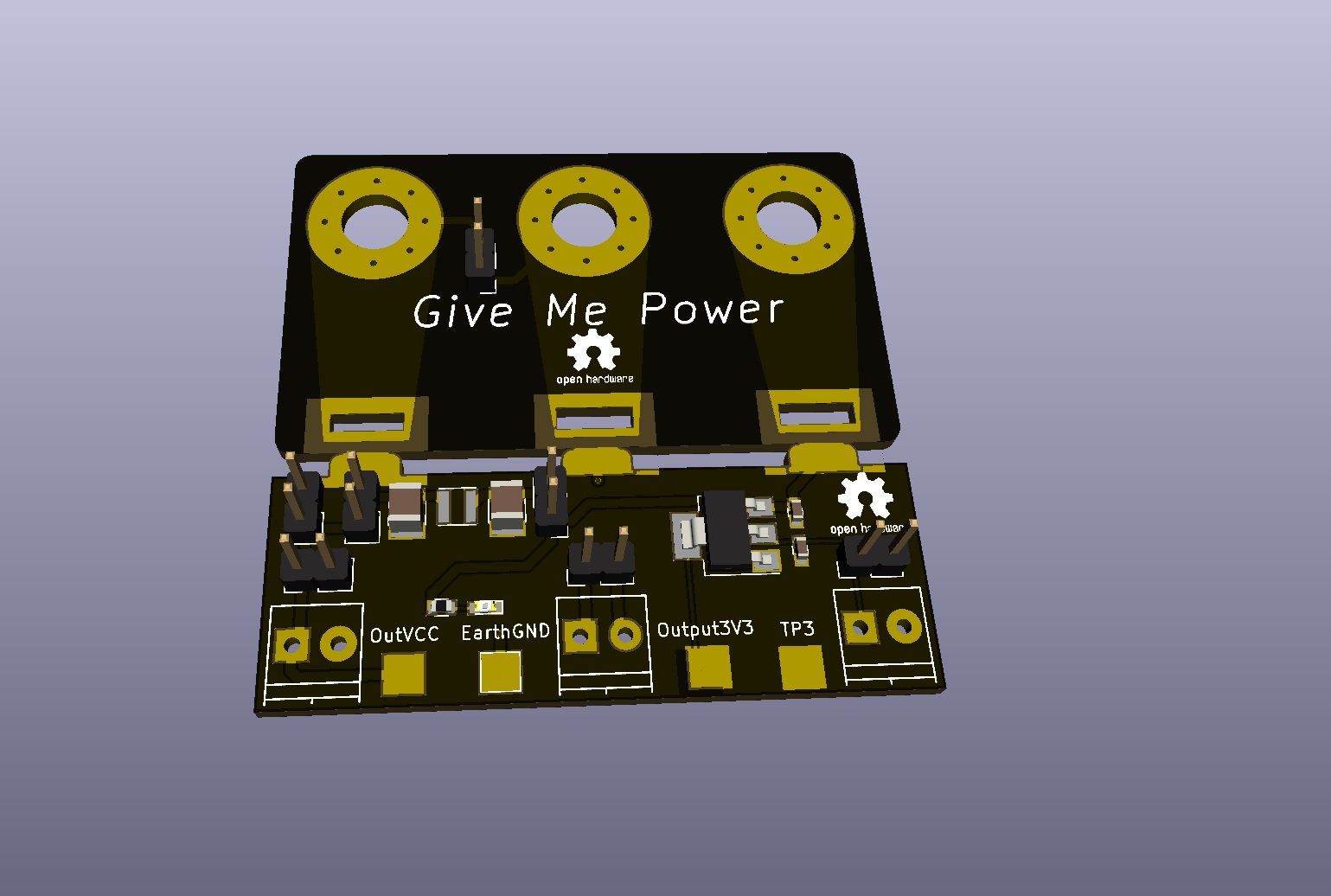
On the subject of having these boards made, I have just send of the Geber files for both Week 8 LoRA Thing and Week 7 GiveMePower hopefully will have those before Christmas. I think I have missed the boat for doing a board for Christmas but defiantly have something in mind for valentines.


AND FINALLY 

I would like to take this moment to say a big thank you to everybody that has encouraged me to do this either with friendly words or likes and retweets. I have I continue to be of some interest and hope that others can learn from my mistakes.

Please continue you support and all updates are on my Git Repo https://github.com/rabid-inventor/board-a-week

Friday 12 October 2018

BAW!! #7 Give Me Power

Sometimes it occurs that the piece of equipment that you are using could be better or have better features maybe adapted to suit your needs better.


This is my bench supply i'm currently using, it work fine on the fact that it supplies power to whatever om working on but it has a few quirks which quite frankly drive me nuts on a daily basis.

I can't set the output voltage without turning the device on, which means if you have a project wired into the terminals you have to unplug it turn the supply on set the output voltage then turn the supply of wire your project back in then you can power it at the write voltage.

The other thing I would like to have is a dedicated 3.3V supply at the moment my solution to that is using an half broken Raspberry Pi powered from a USB port as my 3.3V supply which to be honest is no the best solution. 

The easiest solution to all my problems would be to invent in a good bench power supply. But that would leave me out of pocket and there would end up being a power supply sitting on the shelf unused. 

So lets look at designing an add on board to make it more useful. 

The functions I want to add are:
  • The ability to set the voltage without having to disconnect from the supply.
  • A dedicated 3.3V supply, preferably a linear regulator of up to 1A current supplying.
  • A select-able low pass filter for low noise applications.    
  • An auxiliary channel for current measurement.
  • Hooks for attaching oscilloscope probes. 

The schematic is pretty straight forward not much in the way of active components just lots of connections.


I'm still working with KiCAD finding easier and easier to use each time I complete a board I seem to find a new feature. I this case i was coming to the end of routing the board and there seemed to be a connection missing between EarthGND terminal and a a pin header which is used to link EarthGND to supply ground if necessary. I had managed to label the pin connector as EarthGround instead of EarthGND I was on the final trace and wanted to finish routing the board. 

This is when is discovered that it is possible to change the net of the pad in the layout editor, bonus!!! It mean ti could finish the routing straight away without having to go back to the schematic and change it reexport the net list then re-import it in the board editor.

This is not the 'proper' way to do things because it them means the schematic still has the error and would have to be updated at a later date. But in a pinch it seemed to work. 


Something I have always done is to print a paper version of most boards I design and this one was no exception. As I was designing to fit to another device it was important I hadn't made a mistake.   


To my relief it appears to fit well. So it means there a high possibility the finished board will fit nicely also. 


All done and routed ready for the next one.

Saturday 15 September 2018

BAW!! #6 Blink AN Led competition: BlinkIR

Ok time to really go for it, I discovered that Mouser an electronic component distributor and Macrofab an electronics manufacture with a down to earth approach, are running a competition to design a board to blink a LED, called Blink An LED.

I'll try to post as much of the process of concept and design as I go, the full posts, files and documentation is available at  HackADay.io also this project will have a separate repository for the time being until iIadd the finished version to the main board a week repo.

I finally have the boards and making them up slightly outside of the competition deadline, finally made some up.


The biggest relief was getting them to program. 


And then them blinking. 
I will pull this project into the main Board a week repo as soon as I can. In the meantime the project can be found here:

And the full write up here:


Wednesday 29 August 2018

BAW!! #5 Lets try a new IC (Part 2 Rushing to finish)

Sometimes I find its less about pretty and more about speed. As mentioned in the previous post the BMA400 is a brand new device not even available but having a board ready to receive it can be a big advantage of bring a product to market.


Certainly not the prettiest board I have designed and i was have some difficultly get the Silkscreen Graphics how I wanted it. 

But just over two days it was finished. I normally take the time to sit with a board just to make sure i haven't made a mistake. But there is one great big one on the silk screen.

The design files can be found at:

Feel free to download, clone and remix how you want :) I'd like to know what you get up too.


Sunday 26 August 2018

#BAW!! Weeks 5 Lets try a new IC (Part 1 finding the data)

Still running quite far behind the Bubble watch from week 4 is still an in progress project I'll keep everyone updated as I get more work done on it.

Sometimes a change is as good as a rest so its now time to try a new approach. What about a new IC at this point i'm going to pick something new from Mousers website ( mouser is a component disributer I like their new product search )

First item i have found on the page is a new accelerometer from Bosch Sensortech according to the page it was shown of at the most recent CES and receiving awards for innovation. This is many due to its ultra low operating of around 8uA (super low) thats about 20 time lower than their other Accelerometers at around 150uA operating current.

Its always funny with brand new IC products the offer very little information to even Bosch-Sensortec's own page has very limited technical detail. 

These are the only two documents available at this moment in time:  

A nice give away is the schematic on the shuttle board document which shows how the device is decoupled, and give an idea of how its supposed to be connected as typical application.


Another thing to do is look at the previous generation of the device. At the moment Bosch manufacture the BMA280 which is the previous accelerometer device from them.

I took a look at the datasheets of other Bosch devices and discovered the register map for the device are for the most part identical. This will be a good reference from bringing up this device. 

Time to start making a symbol for the part. I have the Pinout.


I draw it into the KiCAD symbol editor I also find it useful to make sure the do not connect pins are drawn in they can be useful for reference later and making sure the footprint is correct. KiCAD can suggest the correct footprint based on the number of pins so it useful to have everything in front of you.

Time to work on a footprint for the part. I am using the datasheet for the BMA456 being one of the more recent accelerometers i can use the application notes to help draw in what I need for this board.    

schematic is now done leaving enough landings for pull up resistors and jumper links to select the different communication modes. The BMA400 supports both I2C and SPI protocols and there is also an I2C address select. 


Saturday 11 August 2018

BAW!! #4 Bubble Watch Part 1 (Falling Behind)

It another week back into KiCAD but this week want to make a board using Retro Bubble Displays from HP.


These little displays are no longer made unfortunately but I have a few knocking around and really love them. They are  HP QDSP-6064 LED displays and where use in calculators around the 70's and into the early 80's. These displays really pretty and have wanted to do a project with them for long time.

So my idea is to try and do a watch, but better i want to get a modern MCU on there and have a debugging watch. something that is can use to send UART or I2C communications in a hurry.

There is one example of a bubble watch based on an the Texas Instruments MSP430, by solderbug.

I'd like something more capable than an MSP430 with an integrated RTC so i don't have to add more components than necessary. I'm looking at using on of the ST  Microelectronics STM32F030C8. I packs a lots of power with a Cortex M0 32-Bit, with lots of peripherals. I comes i'm at around the £1.50 mark which is pretty good for amount of functionality. My only concern is its size   in a 7x7 mm QPF package its going to take quite a lot of  board space.

So i don't have much room to play with if this was going to be a single sided board, I also have to give room for a power supply. I want to get away form lithium-polymer cells (LiPo). If i was to use one then I have to look at how do I protect the battery from over discharging and how do i fit in a charge circuit while not costing the earth.

I have decided to go with a more humble pair of LR44 coin cells and using a boost converter to bring the voltage up. I think i will have to do some clever sleeping with the MCU to get the best out of this, but as the boost converter will run down to 1.2V input I sound get the most out of this format. Also going to have the battery voltage monitored by the MCU so it can issue a warning to change the battery, and as it is two cells in parallel it will be possible to change 1 cell at a time.


The MCU has a an RTC that can be used to wake up from standby mode. I fact there is no reason that when the display is bing looked at that the device has to be in any run mode at all. 

This means the device and display could be drawing less than 10uA. :) (I'm this mode the device could run up to 11,000h hours).

So far at writing this I have the base power board routed and ready to go.

I unfortunately I am only just finished with routing the base/power board. I'm pretty happy with it, the LR44 cell holders are taking the majority of the board area but I have managed to find a little room for the boost converter.


My problems are to do with the display board. The number of through hole pins are making it difficult to put the board into a format that I'm happy with.

  
  I was hoping i could somehow fit the MCU directly under the display, and as yet have not room for any IO breakout to allow add on modules. 

I think my approach is to put SMT landings for the bubble displays and modify some DIP 12 sockets to be able to solder them onto the pads. I thank i'm going to take the same approach with the crystal and SWD header. 
After a very quick search it seems SMT DIP sockets are freely available. 

This is how far the project is a the writing of this blog I'm going to push ahead to try and complete it had hope that I can not fall too far behind with boards to follow. 

I think my problem is this was quiet a complex project to try and complete in a week. and with this design change its set myself back a little. What this project is teaching me is sometime a redesign is what is needed and I have to just get on with it.

I hope to follow up soon with this design finished. Please let me know what you think, any comments are always welcome thank you to everyone who has given me feedback. 

Wednesday 1 August 2018

BAW!! #3 Into KiCAD and RabidCHARLIE

Board A Week, Week 3 Into KiCAD and RabidCHARLIE

When designing PCB's there several software packages to choose from, these can range from free Open Source options all the way up to full fledged highly integrated software suits. My normal choice for PCB design is Autodesk Eagle, the freeware version I use at home is a great tool but limited by number of layers and board size. More info in the different versions of eagle can be found here.

When starting Board A Week I said one of the things I wanted to try was to use other design tools on of the other design tools I wanted to really give some time to is KiCAD.

KiCAD is an integrated design suit with schematic editor, layout editor and 3D viewer, I have wanted to give KiCAD a try for many years but previous attempts have been unsuccessful. The unfortunate true when you have worked with a certain piece of software for years its becomes quiet difficult to learn a new way of doing things, and consequent have returned to eagle where I'm familiar.

So lets jump into it :


I started of by you throwing down a few parts into the schematic editor and trying to understand how the schematic editor relates to the layout editor using the classic 16 x 2 Character display and an ATMega32u4 MCU. I was thinking along the lines of making some kind of industrial looking watch.

I got to a point that I realised this board would be far too complex to complete before the week was up, especially as I was still getting used to how the KiCAD operates.

I have left my first design as I left it in the GitHUB Repo I don't believe i'm deleting failed attempts as they help me to learn from my mistakes.

So in the end I restarted the board and idea to something useful and simpler a board with Charlieplexed LEDs. Charlieplexing  is a method of multiplexing LEDs by using there diode properties (only allowing current to flow in one direction. This little board could be good for testing IO speed on different devices.


KiCAD  has a very particular workflow that must be adhered to when going between working with the schematic and working with the board design.

  1. Work/Create/Modify Schematic
  2. Assign Foot prints to parts
  3. Export Netlist (important this is done after assigning footprints)
  4. Open Board layout 
  5. Import Netlist (make sure the import options are set correctly whether you want to over write footprints or remove parts that have been removed from the schematic etc.)
  6. If something is wrong repeat from step 2      


The routing tools are much the same airwires are draw between connected pads and you have to connect them with wires. In KiCAD the airwires are always up to date as well, in eagle unfortunately you have to keep hitting the restnest button to get an up-to date render of the airwires which can get annoying when trying to layout the parts in a convenient way.   


The silk and artwork import tools are amazing they import as a library item making them easy to move around.


The Gerber export was really straight forward and had valid Gerbers at the click of a button. Then wrapped them up in a zip file and put them into the Eurocircuts board viewer. Perfect!!!

All in all really happy with using KiCAD its powerful and precise and i think there is a lot more to learn with it. Next weeks project involves making a custom part so some new skills to look at with the software.


Tuesday 24 July 2018

BAW!! #2 TINYMCU

I have always love Micro-controllers (MCUs') I find the fascinating the idea that there is a complete computer on one thin slice of silicone, including RAM, storage and peripherals. And these device can be small super small in fact.

On MCU I have had my eye on for a while is the Atmel Attiny10. Well I'll correct myself its now the Microchip Attiny10 as Atmel where bought out by Microchip a couple of years ago.

Name
Value
Program Memory Type
Flash
Program Memory Size (KB)
1
CPU Speed (MIPS/DMIPS)
12
SRAM Bytes
32
Capture/Compare/PWM Peripherals
1 Input Capture, 1 CCP, 2PWM
Timers
1 x 16-bit
Number of Comparators
1
Temperature Range (C)
-40 to 125
Operating Voltage Range (V)
1.8 to 5.5
Pin Count
6
Source taken from Microchip.com


Though after starting this project I discovered the PIC10F320 and PIC10F322 have the same package and pint layout. Well at least for the SOT23-6 package. 


In the schematic I have decided to add as much debug/experimenting hardware as possible so to do this I have: 
  • Added a jumper to enable the pull-up resistor for the reset pin (incase i would like to use the 4th IO line)
  • Current limiting resistors on all the IO lines ( Just good practise to avoid drawing too much current from such a tiny device each IO allows a maximum of 40mA per pin)
  • Indicator LED's (so I can get instant feedback on the pin status)
  • Jumpers to enable and disable LED's ( I have made these pin jumpers so I can use the raw pins if needed for the ADC and CLK lines if needed.)
  • Programming Header (make life easy)
  • Power indicator LED (Got to make sure there is life :) )
  • No Voltage regulator ( i want to be able to set my own voltages I would love to see how the device performs at the low end of its voltage range)


Don't forget all schematics and design files can be found at https://github.com/rabid-inventor/board-a-week  


Once I started to route the traces I discovered that the board may be able to have a single sided design. 

I rotated the MCU to try an make routing easier.


It was all going so well when I got to one last airwire. BUT:

Unfortunately the board was getting messier and messier just to make it single sided (see the bottom left corner of the board), and to get any further meant making the board size bigger and routing more around the edge. I was unfortunately time to admit defeat and route the board 2 layer.

20 mins later I had it all routed.


The design is now finished and ready to be sent for production. I'm really looking forward to having this one made, and be able to see what is possible with this tiny MCU.

I have also added a CC-BY commons licence please feel free to take a look and comment. Let me know what you think.


Thursday 19 July 2018

BAW!! #1 XOR

Hi everyone its the first week of Boards A Week and i am kind of excited to get underway.

The first board I want to make is an Exclusive OR (XOR) gate, and XOR gate is one of the basic logic blocks used in electronic design which normal comes as an IC package containing multiple gates like MC14070B. The truth table below shows how it operates.

Truth Table


Input A Input B Output C
0 0 0
1 0 1
0 1 1
1 1 0

The reasons I wanted to design this board is to help my understanding of how complementary logic works by using discreet components, so using resistors and FETs.


The full design files can be found at http://github.com/rabid-inventor/board-a-week. I have tried to include all the source material used, including the fonts I have used for creating the silk screen.  


I'm really pleased with how this little board looks and can't wait to have it made to see if my idea works. 

I can't wait to do more of these in the passive blocks in the future. 


Wednesday 11 July 2018

Board a week !!!!!

One of the hardest things as a maker is to keep motivated to be able to push your skills forward, and being able to make all the mistakes in the world so that you can learn from them.

So to answer this never ending problem and to improve my PCB design and understanding of electronics is I will design one board a week and share it.


These are the rules I'm setting for myself.
  • For a board to be complete it has to be fully routed (which is where all the traces are liked)
  • The DRC and ERC are complete. ( these are the checking tools in PCB design software which help the PCB designer to check if the design and electrical layouts are sound)
  • Silkscreen labels complete.
  • To try some alternative CAD software instead of Autodesk Eagle which i'm reasonably used to.
  • Publish to GIT hub as Open Source Hardware 
I don't intend on having every design made of in some cases even populated but I'm going to try and choose one design from each month to send to production.

I'll be doing a blog post each week, and trying to explain some of my design decisions and some of the methods I have tried to use.

I hope you enjoy this journey with me.

Monday 9 July 2018

New Beginnings

Well what can I say..

Long time no post doesn't really cut it so much.

But here I am again starting to get back into the swing of writing content :)

So let bring you up to date:
  • I no longer have the Shed that I made a few videos in I miss it but times have to move on.
  • I still run a PCB assembly at Pimoroni Ltd. in Sheffield which is still an amazing mix of fun, blood, sweat and tears.
  • I have really been practising coding in C, C++ and python.
  • Trying to get to grips with Bluetooth ( A big complicated beast).

New things for the future:

As normal time is never on my side . I really want to be more focused in what skills i'm improving for myself. The 2 improvements i want to make over the coming year are PCB design and embedded programming.


I have a couple of ideas to keep me motivated, I'll keep you posted.