CHUSBIE552

Showing posts with label PCB. Show all posts

Friday, 31 July 2020

USB-C an Experiment

USB-C is more and more becoming a standard in the maker community for power supply and coms with peoples creations. But there is a catch to this although the USB A plug to USB C plug cable is freely available almost everywhere, the sockets can be a little more daunting. There are not only many to choose for including some with and without through-hole pin the pitch and spacing often means you have to spin a PCB to make them work. then there are concerns with soldering them effectively. 


I started to wonder if this would be possible with a USB-C socket with one edge of the PCB inserting into the USB-C plug connector directly. I did a quick Google search and was very surprised that this seemed as though it hadn't been done before. 😏

Next task was to do a deep dive into the USB 3.1 spec sheet 
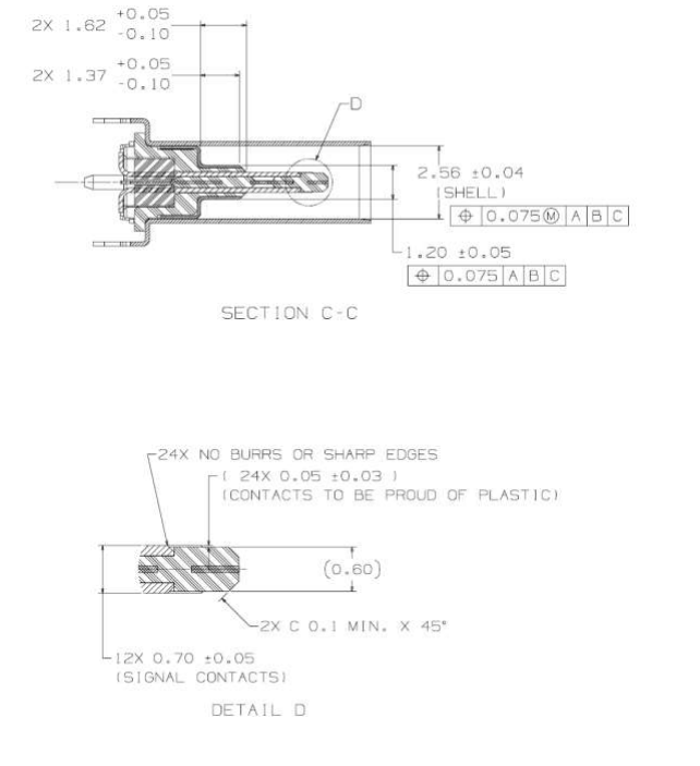
And there it was the "tongue" of the USB-C receptacle is 0.6mm wide wit the contacts proud of the Plastic or in my case PCB. 

Wondered if 0.6mm PCB would break the bank in production costs so it was time to have a search around. My usual stop now for PCBs is JLCPCB. Is I went and had a quick look to see that it wouldn't cost the earth to at least experiment and see if this is viable.
Surprising enough that even with a lead-free finish it would only cost £6 including shipping, at least to do some experimenting.

Even if I ordered V-cut panels which would give me 90+ pieces they would cost less than £0.13 each. 


It was slightly shocked at how the price jumped when I selected my usual black solder mask finish, with a large "Special Process Fee". That would certainly blow the budget feels like I'm ordering boards in 2013 again 😅. Looks as though I want to be able to sell these at a reasonable price then they will have to be green.

With my mind made up it was back to the USB-C spec sheet.
Time to fire up KiCAD and get on with creating the part.

It took a bit of drawing but here is. there is something that I found frustrating within KiCAD. this is I couldn't find a way to draw on the edge cut layer in the footprint editor. Not entirely sure if it is something I missed but decided to draw the board edge into the user drawing layer that I can copy over later.


At the end of the day, I just want to see if this is a workable design so decided that making a breakout is the best plan. 


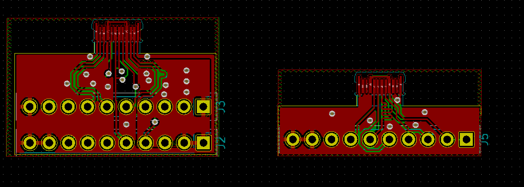
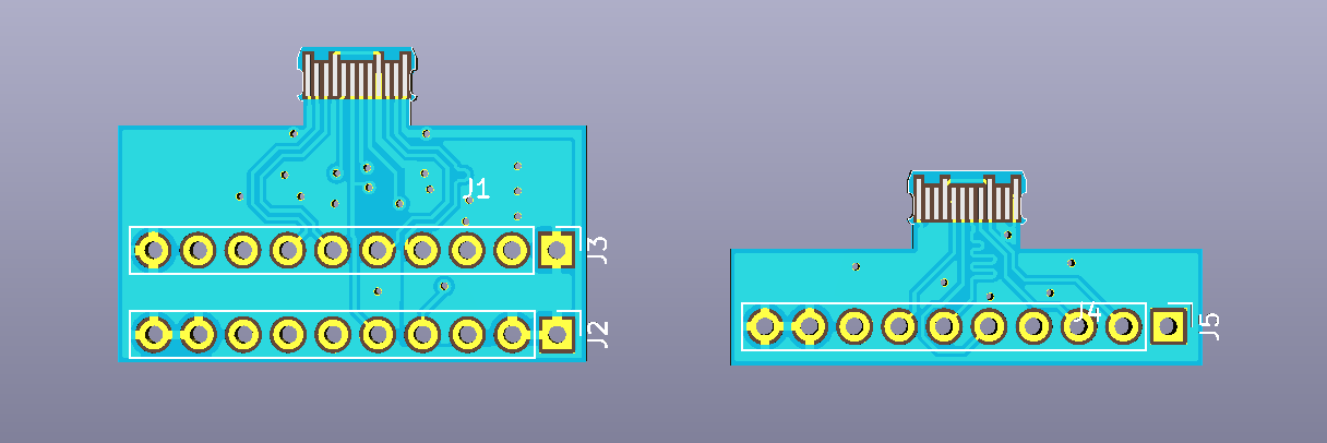
So far I have done two designs the one on the left has all 24 pins broken out for USB-SS and the right one is just for up to USB-HS. All the highspeed lined have their differential traces matched in length but the SS traced don't have the required supporting hardware, caps and filtering etc.

It was around this time i started to tell people what I was up to at which point I found there have been a few previous attempts at this type of connector.


I'm not put off exploring this path however I still think this could be a viable option could do with some tweaks in the long run. The other reason for continuing this is I don't think this option has been completely explored of documented yet.

At this point, I'm making some final tweaks to this design and hopefully sending off for production next month.

If you are interested in exploring this concept yourself all my Kicad files are available on Github so feel free to use them as you desire.

Footprint file: https://github.com/rabid-inventor/Kicad-assets/blob/master/footprint.pretty/usb-c-pcb.kicad_mod

Breakout Design: https://github.com/rabid-inventor/UBSC_PCB_Socket_Adaptor


Tuesday, 28 April 2020

The CH552 MCU

There is a collection of super low cost very capable MCU's on the market but I find myself fascinated with a manufacturer based In china called Jiangsu Heng Qin Ltd. (WCH)

WCH offers a range of hardware including the CH340 USB to UART converter IC the CH438 which is a parallel interface to 8 UART ports and an extensive range of 8 and 32 bit MCU's.


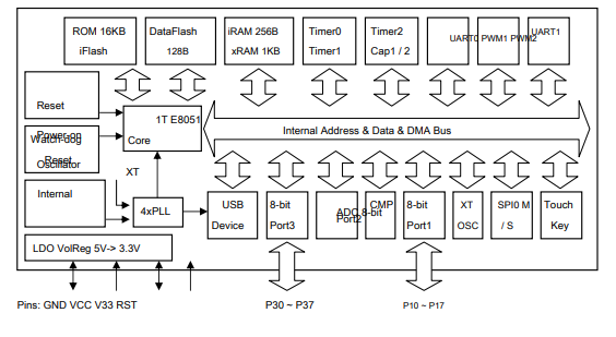
The one I want to look at currently is the CH552 MCU this chip is an 8 bit MCU based on the 8051 instruction set with an E8051 core but the most interesting point is that it has an extensive peripheral set including a USB controller.


These are the onboard peripherals
  • Built-in 16KB Code Flash, 1KB XRAM, 256B iRAM, 128B DataFlash, support byte read and write;
  • Built-in BootLoader, support USB and UART ISP, provide ISP download library;
  • Built-in USB controller and USB transceiver, support USB-Device mode, support USB type-C master and slave detection, support USB 2.0 full speed 12Mbps or low speed 1.5Mbps. Support up to 64 bytes of data packets, built-in FIFO, support DMA;
  • 3 timer / counter, support 2-channel capture and 2 PWM;
  • Provide two full-duplex UART, all support high baud rate communication, UART0 is a standard MCS51 serial port;
  • Provides SPI communication interface, built-in FIFO, support Master / Slave mode;
  • Provides 4-channel 8-bit A / D converters;
  • Supports 6-channel capacitance detection;
  • Supports four reset signal sources, built-in power-on reset, support software and watchdog time-out reset, selectable pin external reset;
  • Built-in 24MHz clock source and PLL;
  • Built-in unique ID number;
  • Package: TSSOP-20, SOP-16, MSOP-10.
There is one downside to how the CH552 operates the 'Code Flash' as they call it is only writable about 200 times. This section of the flash is read only once your program is uploaded. To account for this there is a section of the flash memory called 'Data Flash' this is able to be written over 1 million times which makes it great for storing variables that you wish to keep after the power goes off.


There are many other little surprises as you dig into this component once you start looking into the clock selection register you find out that this little MCU is quite capable of running up to 32Mhz from the internal oscillator.
The device also has a built-in USB and UART bootloader which can be accessed by pulling P3.6 of P1.5 High when the device resets (depending on your configuration).

This chip comes in a variety of packages with different numbers of pins exposed. These include a SOIC16 package the CH552G, a  tiny MSOP10 package the CH552E, and a TSSOP20 package which has all the available IO and functions exposed the CH552T.


Software


There is a header file and examples available from WCH which help to get started including examples of how the USB device works. I would like to in time make this far more user friendly and much more generic.
There are a couple of software stacks fro the device:
https://github.com/HonghongLu/CH554 (for C51 in keil)
https://github.com/Blinkinlabs/ch554_sdcc (for SDCC )

As well as the Official ISP tool there is also an open source programming tool:
https://github.com/rgwan/librech551

The Store

I personally have a lot of love for this little USB hero and want to give it the exposure and credit it deserves. So to that fact, I have decided to stock it on my Tindie Store Rabid's Electronics Emporium.

I also have a Development board range on the horizon called CHUSBIE the I hope that you all grow to like this chip range as much as I do and I will do my best to make it available in many forms and a reasonable cost.
The overlaid packages look a little odd this is so the same PCB can be used for either the CH552T or G. I will keep you up to date on how that goes.

Tuesday, 17 May 2016

Sheds and Circuit Beauty

Arriving on my doorstep was the next installment if my Boldport Club subscription.


The Cordwood Puzzle is Boldport's own tribute to Cordwood circuit design. So time to break my Shed this is part of a new video series 'Rabid Inventor In A Shed'. Everyone needs a workshop-shed so spent some time kitting out mine, and it was about time to break it in.

Its Not Much But Its Mine 

With Integrated Drone Parking 


Saturday, 18 July 2015

Dirty Circuits Done Dirt Cheap


Often design and research is and expensive business, especially when dealing with technology that your are unfamiliar with. A big proportion of this is PCB manufacture and I have spend a few years looking for a low cost reliable method for PCB production.

The most cost effective method is to have the boards produced overseas but then you won't be sure of the quality of the boards until they return. This is where Dirty PCB step in.

Dirty has been setup by the guys at Dangerous Prototypes as a reliable access to PCB fabs overseas.


I discovered Dirty PCB while looking at another PCB manufacturers reviews and recommendation on a forum post.

So went over to there website and I was almost knocked of my feet at how cheap 2 layer PCBs were.


If you can keep your design under 5cm x 5cm and don't mind if you end up with anywhere between 8 - 12 PCBs then it is only $14 (9GBP) that could be less than 0.10GBP   1GBP per PCB. WOW! There is also a selection of colours for the solder masks at no extra cost.

For me that is great for me as most of my designs are under this size as 50x50mm is quite equate for a breakout board but for $11 more you can have up to 10cm x 10cm (100x100mm That's huge). 

There are a few things that you need to accept to get this price level the boards can only be 2 layers and the pad finish will be HASL (Hot Air Solder Leveling) there is an option for ENIG (Electro-less Nickel Immersion Gold) but it is $15 more. Also there free postage option is quite slow so its worth paying $19 more to get DHL airmail, I realise this is more that the PCBs cost but otherwise it could be a up to 8 weeks delivery. 

Next thing to have a look at is there capabilities, this is all listed in the FAQ.

Capabilities
ITEMCAPABILITY
MaterialFR-4 0.6mm-2.0mm 1oz copper ('standard' PCB material is 1.6mm thick, but we default to 1.2mm)
Layer number2L
Maximum size100*100mm (10*10cm)
ShapeAlmost anything! We'll send it and see if they accept it!
Min internal slot32mil (0.8mm)
Min core thickness4mil 0.08mm
Min core thickness16-96mil(inner) 16-118mil(out)
Min w/s5/5mil(I/L)
Min w/s5/5mil(O/L)
Min silkscreen line0.15mm
Min BGA sizeOblong:10*13.5mil/circle:12mil
Min SMD width8mil
Min solder dam3mil(green)/3.5mil(black)
Min dielectric thickness2.5mil
Min diameter of finished hole12mil
Tolerance of drill position+/- 2mil
Tolerance of finished hole sizePTH +/- 3mil
Tolerance of finished hole sizeNPTH: +/- 2mil
PTH hole copper thickness0.6~1.4mil
Max A.R of PTH8:1
Surface copper thickness1oz
Routing dimension tolerance(Z0) Impedance control 4mil
V-cutNow refused! 80*80mm(min) 380*300(max)
(Z0) Impedance control+/- 15%
Ionic contamination< 6.4ugNaCl/inch2
Surface treating(No PB) hot air levelling/AuSn/AgCN/Electrogilding/Ni/OSP*/G.F
*OSPOrganic solder-ability Preservatives
This is much the same as most board houses standard service I'm mainly looking at the trace thickness and clearance which is 4 thou (thousandths of an inch, this is a bit of a legacy thing with board houses) and a clearance of 5 thou.

There is some helpful things further down the page, Dirty PCB supply a design rules check file for Eagle this file is use in you design rules check to make sure your PCB design is manufacturable. They also supply a cam processing file to help export your design manufacture file. But if you use Eagle like I do you can just send in your .brd design file and Dirty PCB will do all the exporting for you. This is great as I don't have to worry about getting the export wrong or sending the wrong layer files.  

So that's it time to give them a spin. Note: Dirty PCB only accept PayPal payments best to make sure you PayPal details are upto date.

On thing I noticed after putting in my order is that the level of communication is amazing are reassuring, and you can also check the status of you order in the websites status page.  

One Week Later (seriously that is really really fast!)


Such Box! Much Cute! 


There is no mistaking this box the end stamp is very cool.


And then you even get a sticker, I like stickers :)


The PCBs where well wrapped but a little loose in the bag the could rub against each other possibly scratch the finish but this didn't happen in my case. 


I always get excited to see one of my own designs as PCB please don't get too excited this is not a product its just a demo board to try out a BLE chip that I might use in a product ;)


The finish is great the Silkscreen is legible and the resist is nice and even. lets have a look under the microscope.


The quality is excellent and precise the soldermask is tight to the pads with none of the ground fill exposed. The thing that really knock me off my feet is they have also managed to apply the mash between the the pads on the main package, these gaps are less than 0.2mm in width that is brilliant.

  
 And for the free sticker.


Got the perfect place for that.

So what do I think of Dirty PCB here is my round up:

  • Easy of use: Straight forward and quite fun the site feels as though it doesn't take itself to seriously and approachable. Though more payment options would be a nice addition.
  • Communication: Reassuringly comprehensive without feeling like I'm being spammed.
  • Lead Time: Quick! 
  • Packaging: Exciting!
  • Finish and Quality: Astounding good.
I can only award Dirty PCBs up to 5 sparks but in may opinion they deserve 6. Very pleased with the service.